Functional structures
Fabrication of functional structures with conductive materials
Printing conductive materials such as silver, carbon, or copper onto flexible substrates enables the integration of sensors into a wide range of everyday objects, opening up new applications in robotics, wearable electronic devices, medical technology, and the automotive industry. The sensors can be manufactured in unconventional shapes and sizes to meet the requirements of specific applications.
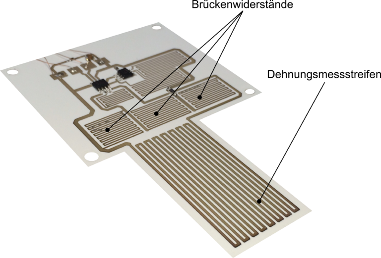
Inkjet printed strain gauge
Printed strain gauges are created by printing conductive materials onto a flexible substrate, such as a film, and are used to measure strains and deformations in materials such as metals, plastics, and composites. Due to their thin and flexible nature, they can be adapted to a variety of surfaces, offering a cost-effective alternative to traditional strain gauges.
Printed capacitive force sensors
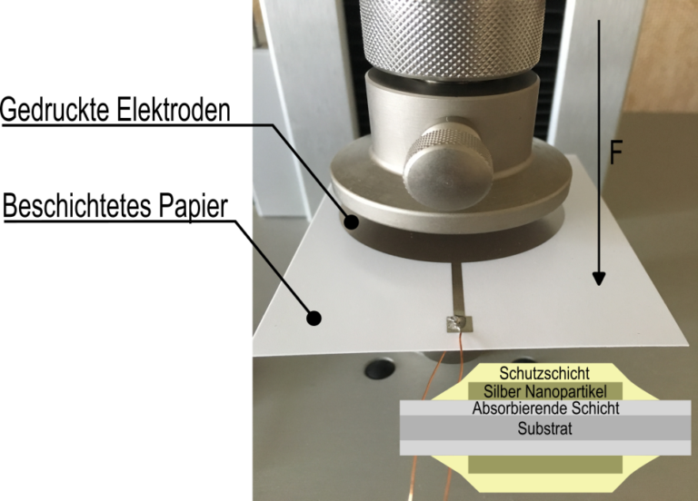
Printed capacitive force sensors are cost-effective and easy to integrate, measuring the force applied to an object. They are created, for example, by double-sided printing on a thin, flexible film, forming a capacitive sensor. The capacitance changes due to the deformation of the film when a force is applied to the sensor. Alternatively, resistive force sensors can be made by embedding conductive particles in elastomers.
Printed strain gauges arranged in a grid
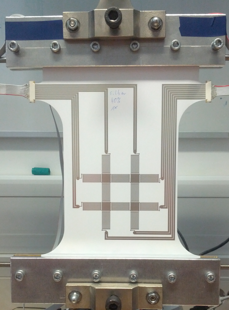
When printed conductive traces are arranged in the form of a Cartesian grid, the deformation of component surfaces can be measured. The conductive traces change their electrical resistance due to mechanical loading caused by stretching or compression. With such a sensor, deformations or defects in components can be detected early on and during operation.
Resistive surface strain sensors
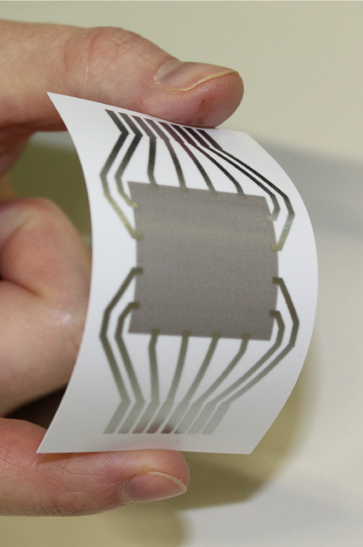
When a surface is fully printed with materials like carbon nanotubes instead of printed conductive traces, the deformation of component surfaces can also be measured. The surface changes its electrical resistance due to mechanical loading caused by stretching or compression. One advantage is the simpler fabrication of the sensor compared to multiple individually printed conductive traces.
Printed antennas
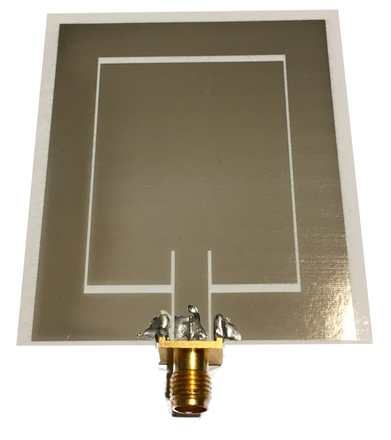
Planar antennas or microstrip antennas can be easily fabricated using additive printing techniques. They are composed of conductive materials such as copper or silver and are printed onto a substrate layer. By adjusting the geometry, properties such as radiation pattern or resonance frequency can be influenced. Printed antennas offer a good combination of efficiency, simplicity, and cost-effectiveness, making them suitable for many IoT applications.
Capacitive touch sensors
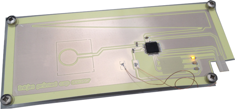
Capacitive touch sensors are used to detect touches or proximity to a surface by responding to changes in the electric field when a finger or a conductive object approaches. They can be fabricated using inkjet or screen printing techniques using conductive inks. These sensors can be used in a variety of IoT applications.
Back injection of printed electronics using rapid tooling
Overmolding, also known as insert molding, is a well-known process in the plastic industry. One application example is the production of decorative interior parts in the automotive industry. In recent years, additive manufacturing techniques have rapidly expanded into the injection molding field. For instance, it is used to produce injection molds made of metal or plastic. This technique is referred to as rapid tooling and can be used to overmold substrates with printed conductive traces and components within a matter of days.
Please note that these examples are just a selection from our development projects. If you have any questions or need further information, please don't hesitate to contact us. We'll be happy to assist you!
